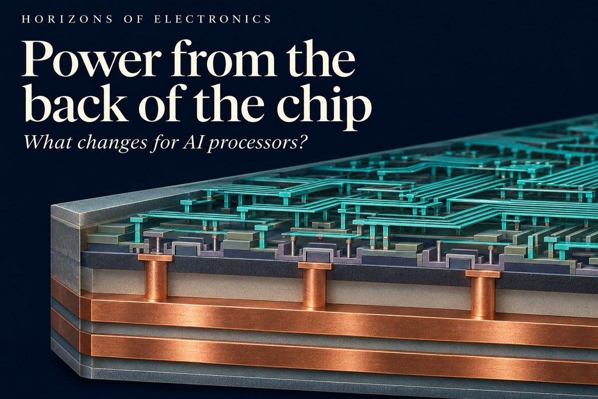
A processor needs a steady voltage at the instant a group of transistors switches. In a densely wired chip, the metal that supplies current competes for space with the wires that carry signals. Moving the supply network to the back of the silicon changes the route electricity takes to reach those transistors.
What difference could that make when an AI processor runs an inference? An Intel experiment on a fabricated processor core gives a measured frequency benefit. A separate study of an Arm core design shows how the choice of power rails changes the voltage lost along the way. Together they explain which parts of a chip can gain operating margin, why clock speed alone cannot predict response time, and what an engineer would have to measure to establish energy per inference. The comparison also helps interpret recent process results that combine backside power with changes to the transistors themselves.
How much voltage reaches the logic?
Picture a group of arithmetic units starting a matrix multiplication together. Current must travel from the supply to those units and back. A conductor with resistance R carrying current I drops a voltage IR. When current rises suddenly, the package and the local supply network can introduce a further transient dip. The lowest voltage at the logic matters because a gate that switches too slowly can miss the next clock edge. Chip designers allow a voltage margin for that possibility. [4]
With conventional frontside wiring, the supply routes share the stack of metal above the transistors with signal wires. Backside power delivery gives the supply its own metal layers on the opposite face. Short vertical connections feed the logic. This opens space for signals on the front and gives designers room for wider supply conductors. The electrical result depends on every part of the new path, including its contacts. [1] [3]
What changed on Intel’s test chip?
Intel built an E-core test chip on its Intel 4 process with FinFET transistors and PowerVia. Compared with a similar core design using frontside power, the team reported a 6% higher clock frequency and a reduction of more than 30% in the size of the platform voltage dip during operation. These measurements describe the test chip; the team did not time an AI inference. [1]
The companion paper reports a frequency gain of more than 5% on silicon. Both papers describe the same development programme. The implementation team also reports that standard cells occupied more than 90% of the available placement area in large parts of the core. That figure tells us how densely the cells could be placed; it says nothing about how often they were doing useful work. [2]
Where does the electrical gain come from?
One way to deliver power from the back is to connect the supply to metal rails buried near the transistors. Researchers fabricated these connections in a thinned wafer and measured how their resistance varied with the metals used for the rails and vias. Those measurements test the electrical path itself. They do not establish how much power a processor using that path would draw. [3]
A Cortex-A53 design study compared nine power grids in three families. The researchers kept the chip area and the 0.7 V supply fixed. Relative to conventional frontside power, they reported a 25% reduction in on-chip resistive voltage drop with buried rails fed from the front, and an 85% reduction with buried rails fed from the back. They calculated these drops from routed designs without running an application workload. [4]
Did lower voltage drop mean lower power? At the same normalised clock frequency (1.4 in the study’s units), the front-fed buried rails used an estimated 10% more power than the conventional design; the back-fed buried rails used 8% less. In the front-fed design, cells needed to connect the buried rails took up space and made the layout harder to route. Voltage drop and power can therefore move in opposite directions. Neither percentage measures energy per inference. [4]
Intel’s original 18A process already used PowerVia. Its 2026 successor, 18A-P, retained backside power while changing the transistors, interconnects and design rules. Comparing those two processes cannot isolate the effect of moving the supply to the back. The earlier Intel 4 test chip offers a more direct comparison for that question. [1] [5] [6]
When would a faster core shorten an inference?
One accelerator might use the extra voltage margin to run faster. Another might keep its clock unchanged and seek a lower supply voltage. The second choice calls for measuring joules per completed inference, including the memory and other components inside the chosen power boundary. Both comparisons need the same model, numerical precision, batch size and output quality. A sustained run should also record temperature and clock frequency once the chip has warmed up. Peak frequency alone leaves those questions open.
To test the effect on inference, run two workloads on each chip implementation: one dominated by arithmetic and one by memory traffic. For each workload, replay identical requests on both chips and compare latency, energy per completed inference and sustained throughput. Estimating cost per inference would also require manufacturing yield, packaging cost and the useful work each system delivers over its lifetime.
Sources and scope
This selective review covers publications examined through 14 November 2026. The evidence includes a fabricated processor core, electrical measurements of interconnect structures, a processor design study and a later process report. None of the cited comparisons measures the same AI inference on two otherwise matched accelerators with frontside and backside power delivery.
- Intel PowerVia Technology: Backside Power Delivery for High Density and High-Performance Computing. 2023 Symposium on VLSI Technology and Circuits. Fabricated test core and frontside comparator.
- E-Core Implementation in Intel 4 with PowerVia (Backside Power) Technology. 2023 Symposium on VLSI Technology and Circuits. Companion report on layout, frequency and thermal behaviour.
- Buried Power Rails and Nano-Scale TSV: Technology Boosters for Backside Power Delivery Network and 3D Heterogeneous Integration. 2022 Electronic Components and Technology Conference. Measurements of rails, vias and contacts.
- A Holistic Evaluation of Buried Power Rails and Back-Side Power for Sub-5 nm Technology Nodes. IEEE Transactions on Electron Devices (2022). See the abstract and conclusion for voltage drop, and section IV-A, figure 2(a–b), for the power comparison and the nine grid designs. Open manuscript.
- Intel 18A-P CMOS Technology Enhancement Featuring Advanced RibbonFET (GAA) Transistors and PowerVia for High-Performance Computing. 2026 Symposium on VLSI Technology and Circuits. Process comparison with Intel 18A. Official symposium programme.
- Intel 18A platform report. 2025 Symposium on VLSI Technology and Circuits. The original description of the 18A process identifies PowerVia as part of the baseline.
Liked this post? Follow this blog to get more.