A blue pixel should send as much light as possible towards your eye. A power supply in an AI server should deliver as much of its input power as possible to the electronics. Both can use semiconductors from the gallium nitride family. Where does the energy go in each case, and how much still becomes heat?
The pixel offers a fair way to ask the question: hold the light output per unit area fixed, then measure the surface temperature. On a server power board the test is different. Engineers measure the electrical power on either side of a converter. A third experiment has put complementary nitride transistors together to switch a logic signal and store a bit. The three results tell us which jobs gallium nitride (GaN) can take on, from producing blue light to performing a function usually assigned to silicon. [1] [2] [3] [6]
Where does a blue pixel lose energy?
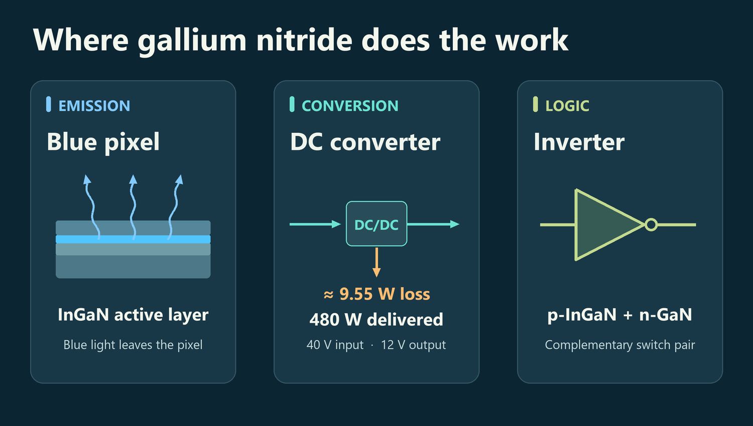
Gallium nitride belongs to a family of wide-bandgap semiconductors. In a blue LED, layers containing indium gallium nitride (InGaN) provide an active region where electrons and holes can recombine and release photons. Some carriers lose their energy through other routes. Defects along the etched edges of a small pixel are one such route, and the energy can ultimately warm the device. In an LED-backlit liquid-crystal display a separate layer modulates the light. In an emissive micro-LED display, the tiny emitter can itself form the blue subpixel. [1] [2]
Baek and colleagues changed the layers that confine and supply carriers in blue micro-LEDs. They compared devices at the same optical output per unit emitting area, 1 W/cm², and mapped the surface temperature from changes in reflected light. The improved structure gave a lower average pixel temperature. This comparison matters because a cooler but dimmer pixel would answer a different question. The team also reported 3.00% external quantum efficiency at a current density of 0.1 A/cm² in a device measuring 10 × 10 μm with treated sidewalls. That figure counts photons escaping per electron injected. Converting it into an electrical energy efficiency would also require the photon energy and the electrical input. [2]
What can GaN replace on a server power board?
Follow the power before it reaches the processor. A converter may step an intermediate bus down from 48 V to 12 V. Further regulators supply the lower voltages needed by the chips. In a switching converter, transistors repeatedly connect and disconnect current paths while inductors and capacitors store and release energy. A GaN power transistor can take the place of a silicon power MOSFET in a stage designed for its electrical characteristics. Energy is lost through resistance during conduction and while voltage and current overlap during switching. How much depends on load, frequency, gate drive and layout. [3] [4]
Reusch, Strydom and Lidow tested this substitution directly. Their two resonant converters used the same topology, transformer core and windings, with similar transistor on-resistance. Both converted 48 V to 12 V and switched at 1.2 MHz. The GaN version gained about one percentage point in peak efficiency over the silicon version. Figure 8 gives another way to read the result. With a loss budget of about 12 W, the authors estimated about 270 W of output for the silicon design and 325 W for the GaN design. Those figures belong to these two prototypes. They show how a designer can spend the thermal margin on more useful output. [4]
How much heat is left at 98% efficiency?
Texas Instruments tested a separate GaN-based converter intended for intermediate power distribution. At 40 V input and 12 V output it delivered 480 W at 98.05% efficiency. Dividing the output by 0.9805 gives approximately 489.55 W at the input. The difference is about 9.55 W lost in the measured converter. That is a calculation from the reported electrical data. It includes the auxiliary supplies and excludes the output connector loss. The switches, magnetic components and other parts share that loss. The design provides for a heat sink and a fan. [3]
The operating point matters. With 48 V at the input, the same board peaked at 97.78% efficiency at intermediate load and reached 96.82% at full load. Peak efficiency alone cannot predict a server’s electricity use across an afternoon of short requests and idle periods. The load curve determines how much power is lost before electricity reaches the computing hardware. The processor then generates heat of its own. [3]
There is also a difference between generating less heat and carrying existing heat away. At EPFL, researchers integrated microfluidic cooling channels into the substrate of GaN-on-silicon electronics, bringing coolant near the heat source. The nitride layer provided an electronic function, the silicon supported the structure and the fluid transported heat away. This is one practical reason the two materials can appear in the same device. [5]
How far has GaN gone inside a logic chip?
Complementary logic needs useful switches of both polarities. Producing a strong p-type channel, in which holes carry current, has been a particular difficulty in GaN technology. In 2026 a Peking University team and collaborators used the built-in electrical polarization at nitride interfaces to integrate a p-channel InGaN transistor with an n-channel GaN transistor. They made inverters, logic gates, a ring oscillator and a six-transistor static memory cell. At 6 V, a five-stage oscillator ran at 9.6 MHz, corresponding to a signal delay of 10.4 ns per stage. The researchers also tested the inverter up to 200 °C. This temperature describes the environment in which it retained its switching function. Heat generated by the inverter itself would require a power measurement. [6]
The same team integrated control buffers with high-voltage GaN power transistors. That gives the logic result an immediate engineering purpose: put the driver near the switch it controls. Extending these elements into a general-purpose processor or AI accelerator would require dense logic, large reliable memory arrays, interconnects and competitive energy and yield across a die. The study tested building blocks. Our earlier article on silicon nanosheets follows the separate problem of controlling a short channel in a production logic technology. [6]
A separate 2026 demonstration shows how the two materials can share the work of controlling a power supply. On a 300 mm wafer, researchers integrated n-channel GaN switches and p-channel silicon transistors in the same process. They built a 32-bit serial interface for configuring on-chip circuits and a ring oscillator with 7,213 stages. The interface demonstrates a working control function. The oscillator shows how far the researchers could scale a chain of gates. Measuring any benefit to an AI server would require running its power supply under a representative load. [7]
What would an AI operator notice?
A more efficient power stage can reduce the electricity needed to deliver a given accelerator workload, even if the model returns its answer at exactly the same speed. A fair server test would meter energy at the server inlet and at the converter output over the same workload, including idle and burst periods. Match the model, output quality, concurrency, latency and cooling conditions. Report joules per generated token and the share lost in conversion. Any claim about facility-wide cooling savings also needs a measurement of cooling energy outside the server. The strongest case for GaN today is specific: emit blue light, switch electrical power with lower losses in demonstrated designs, and bring small logic functions next to power devices. The evidence for replacing a silicon AI processor is still at the circuit-building-block stage.
Sources and scope
Evidence reviewed through 17 November 2026. The thermal map, the silicon–GaN comparison, the converter efficiency curve and the experimental logic circuits come from different devices. The sources below identify the limits of each measurement.
- Royal Swedish Academy of Sciences (2014). Scientific Background on the Nobel Prize in Physics 2014. Nitride semiconductors, efficient blue LEDs and display applications.
- W. J. Baek et al. (2023). Ultra-low-current driven InGaN blue micro light-emitting diodes for electrically efficient and self-heating relaxed microdisplay. Nature Communications 14, 1386. External quantum efficiency and surface temperature at matched light output per unit area.
- Texas Instruments (2025). 48V–12V GaN-Enabled 1.1kW, Two-Phase Buck Converter, One-Fourth Brick Power Module Reference Design. TIDA-050089, design guide TIDUFF3. Figures 3-3 and 3-4 give the measured curves and the text specifies the power measurement boundary.
- D. Reusch, J. Strydom and A. Lidow, Efficient Power Conversion (2013). Improving System Performance with eGaN FETs in DC-DC Applications. 46th International Symposium on Microelectronics. Figures 6–8 compare the two physical resonant converters.
- R. van Erp et al. (2020). Co-designing electronics with microfluidics for more sustainable cooling. Nature 585, 211–216. Integration and experimental evaluation of near-junction cooling.
- Peking University and collaborators (2026). Monolithically integrating polarization-doped InGaN p-FET and GaN n-FET for complementary logic circuitry. Science Advances 12, eaec4563. Figures 3–5 cover the inverter temperature test, oscillator and static memory cell.
- S. J. Bader et al. (2026). A 300mm Monolithic GaN MOSHEMT and Si pMOS Technology Demonstrating Energy-Efficient Multi-Thousand-Gate Digital Logic for Power Management. IEEE/JSAP Symposium on VLSI Technology and Circuits, JFS6.3. Official technical programme and abstract.
Liked this post? Follow this blog to get more.