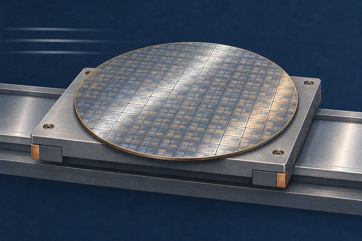
A silicon wafer rides on a moving stage while a lithography scanner projects a circuit pattern onto its surface. With each change of speed, the machine has to manage both the energy of the moving stage and its position. Where does the energy go when the stage brakes for the next exposure?
In Canon’s FPA-6400ES6a, some of it comes back as electricity. Canon says that the new scanner uses less electrical energy to expose a wafer than its previous model fitted with the Grade 10 upgrade. For a factory supplying memory for AI accelerators, the question is how much of that saving survives the journey from one exposure to a memory die that passes its electrical tests. [1] [2]
One braking cycle
The drive draws electricity to accelerate the stage. The moving assembly then has kinetic energy, proportional to its mass and to the square of its speed. When the drive exerts a force against the motion, it can convert some of that energy back into electrical energy. Canon’s system stores the recovered energy until it is needed again. On a later demand for power, that stored energy can supply part of what the machine would otherwise draw from the mains. Some energy is lost during conversion and storage. [1] [2]
The manufacturer also redesigned the power supply. Its Japanese announcement attributes lower electricity consumption per wafer to the new system as a whole. It gives neither the number of kilowatt-hours saved nor the share attributable to braking. The mechanical challenge has its own measure of success. Accelerating and decelerating the stage can set it vibrating. Canon credits a new vibration-suppression system with helping the next pattern land in the right place. [1] [2]
What 400 wafers an hour counts
This scanner uses 248 nm light from a krypton fluoride (KrF) laser to expose a pattern in a light-sensitive coating. Canon rates it at 400 wafer passes per hour for 300 mm wafers with 96 exposure fields per wafer. Its Grade 10 predecessor was rated at 300 under the same field-count and wafer-size conditions. That is one-third more wafer passes per hour at the rated cadence. Each wafer still has other patterned layers to acquire and many processing steps to complete. [2] [3] [4]
A sharp pattern still has to land on its contact
Imagine exposing the opening for a connection to a metal line in the layer below. Resolution determines how fine an opening the scanner can draw. Overlay describes how closely the opening lands on its intended position. An opening with clean edges can still miss part of its contact. Canon specifies resolution of ≤90 nm and overlay of ≤4 nm. Its optional alignment light helps the scanner read existing marks under different film stacks. The Grade 10 model already offered 4 nm in an optional single-machine overlay specification. [2] [3] [4]
The direct ASML comparison is the TWINSCAN NXT:870B, another KrF scanner. ASML specifies at least 400 wafers per hour and resolution of ≤110 nm. For overlay it gives ≤6 nm between matched machines and ≤4 nm on product in specified cases. Those figures establish the same nominal throughput threshold and a finer published resolution for Canon. Deciding which places contacts more accurately in a given memory process requires measurements on that product. A factory can use KrF for layers within its reach while reserving extreme ultraviolet lithography for more demanding patterns. [5] [6]
From a wafer pass to memory for AI
During language-model inference, an accelerator repeatedly reads model weights and other data. High-bandwidth memory (HBM) puts stacks of DRAM dies close to the processor to supply those reads. Micron’s HBM4 for NVIDIA’s Vera Rubin platform gives a concrete example. More usable DRAM dies leaving a factory can support more HBM stacks if the stages that join, package and test them can keep pace. The scanner’s electricity is spent during manufacture. Energy used later to answer a prompt belongs to a different measurement. [9]
Canon reported growing sales of KrF scanners for memory applications before announcing the FPA-6400ES6a on 10 November 2026. It scheduled the commercial launch for early December. The public documents cited here leave the first qualified memory product and its production yield open. Canon’s separately reported objective of adoption in volume manufacturing from 2027 concerns nanoimprint lithography, which uses a patterned mould. [2] [7] [8]
A memory manufacturer could test the benefit by running matched lots through the same layer at the same exposure dose and field count. Meter electricity at the scanner inlet, record idle time and auxiliary loads, then measure overlay after etching and count the dies that pass electrical test. If this exposure is the bottleneck, faster scanning can release capacity. If stacking already limits output, the exposure can still save electricity while finished-stack deliveries hold steady. The result to look for is how many electrically sound memory dies a shift delivers, and how many kWh it takes to deliver them.
Sources and scope
Evidence reviewed on 16 November 2026. Scanner ratings are manufacturer specifications. The electricity example uses normalized units. The proposed memory-line comparison identifies measurements a customer could make.
- Canon (10 November 2026). FPA-6400ES6a launch announcement, Japanese edition. The energy section and note 4 identify the wafer exposure and the Grade 10 comparison.
- Canon (10 November 2026). Launch announcement, English edition. Stage motion, vibration suppression, alignment illumination, exposure conditions and planned availability.
- Canon. FPA-6400ES6a technical specifications. Exposure wavelength, resolution, overlay and wafer size.
- Canon (13 June 2022). Grade 10 productivity upgrade for the FPA-6300ES6a. The reference scanner, its 96-shot recipe and the optional single-machine overlay specification.
- ASML. TWINSCAN NXT:870B. KrF source, resolution and rated throughput.
- ASML (29 January 2025). Quarterly results presentation, slide 9. The two overlay figures refer to different tests.
- Canon (2026). Interim report for the 126th business term. Demand for KrF lithography systems for memory applications.
- Canon (2026). Third-quarter results presentation with notes, p. 12. The 2027 mass-production objective concerns nanoimprint lithography.
- Micron Technology (16 March 2026). HBM4 in high-volume production for NVIDIA Vera Rubin. A production example of the memory used in AI accelerators.
Liked this post? Follow this blog to get more.