A logic cell needs two kinds of wire. One brings power to its transistors. The other carries a signal, perhaps a bit from a multiplier to the next stage of an AI accelerator. Both have to fit. How can a chip designer make room for more connections while keeping the same density of transistor gates?
TSMC’s A16 process offers one answer. Its Super Power Rail brings the supply to the device through a direct contact from the back of the wafer. At the 2026 Symposium on VLSI Technology and Circuits, TSMC reported that A16 preserved the gate density of its N2P process while increasing chip density by 8–10%. The distinction becomes easier to see if we follow the last part of the electrical path. [1]
Where does the supply meet the transistor?
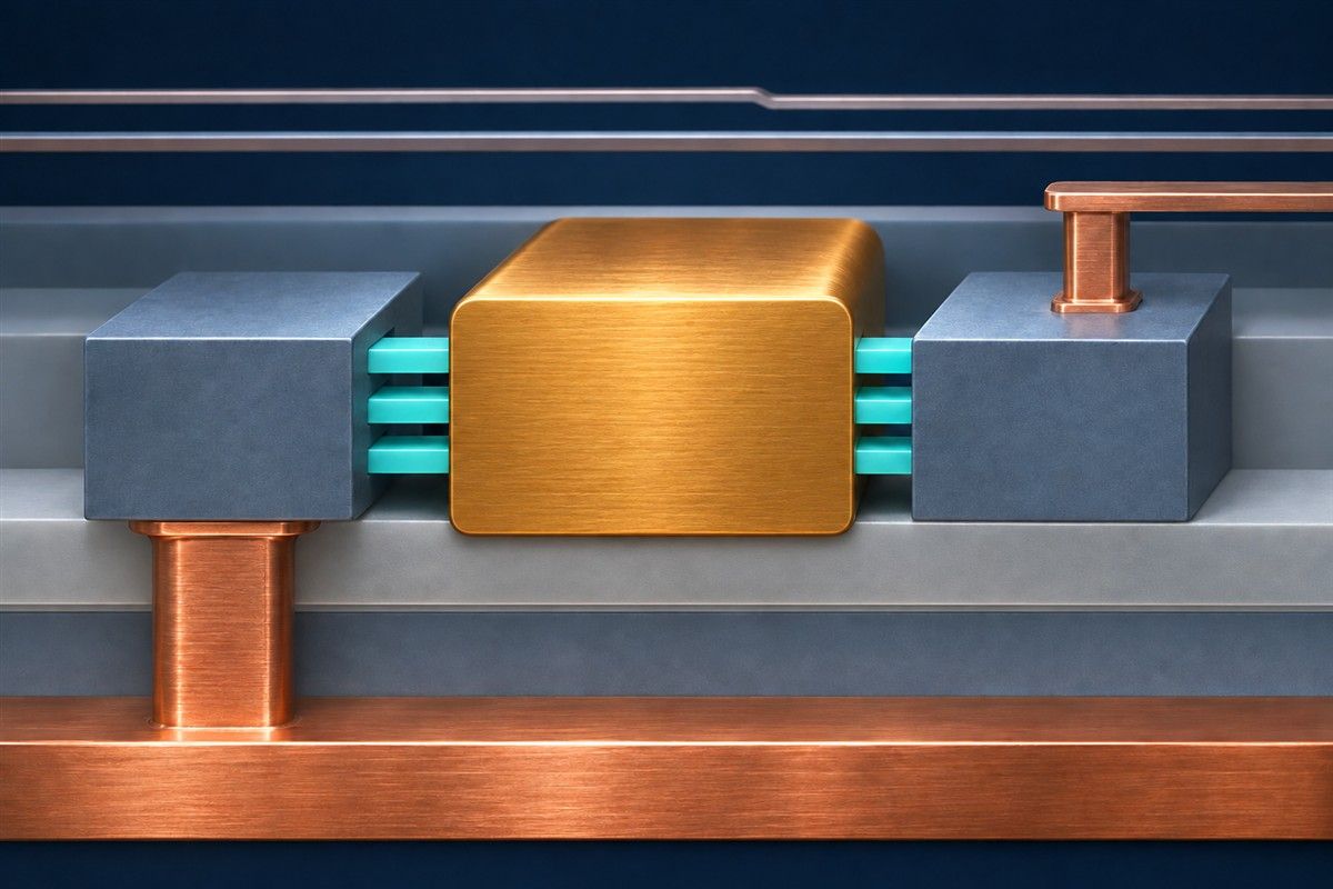
A nanosheet transistor has thin, flat semiconductor channels stacked one above another. Each sheet joins two terminal regions called the source and drain. A conducting gate, separated from the channels by an insulating layer, wraps around the sheets. Changing the gate voltage changes how readily current can pass through them. The transistor family used in N2 already had this gate geometry. A16 combines an enhanced nanosheet transistor with a different way to reach the power-connected terminal. [1] [3]
Consider a simple inverter as it drives its output high. In that state, its upper transistor conducts and charges the output through a path from the positive supply. In a direct backside design, the rail can reach the supply terminal from underneath the transistor. The input still controls the gate, and the output still connects to the next cell. Moving that supply connection frees space in the front-side wiring that the designer can use for signals. The exact shape of a manufactured contact depends on the process. [1] [2] [4]
How can the chip get denser if the gates do not?
The gate density describes one part of a design. A working block also needs room to connect its cells. Imagine two layouts containing the same logic. If one needs extra space between rows to route its signals, it occupies a larger area even if its transistors are laid out at the same pitch. A supply contact that removes a routing obstruction can therefore improve the density of the connected block. TSMC identifies complex signal wiring and dense power networks as the intended use case. [1] [2]
What was held constant in TSMC’s comparison?
Both documents compare A16 with N2P, the performance-enhanced member of TSMC’s N2 family. In April 2024, TSMC projected 8–10% higher speed at the same supply voltage, or 15–20% lower power at the same speed. For data-centre products, it gave a chip density of up to 1.10 times the N2P figure. [2]
In June 2026, the technical team described the platform as qualified and reported 8–10% higher speed at equal power and an 8–10% gain in chip density. Holding voltage constant can leave power free to change as a circuit switches faster. Holding power constant sets a different constraint. The two speed ranges come from the same manufacturer under differently stated conditions. Speed and power gains represent alternative operating comparisons, so adding the percentages would have no physical meaning. [1] [2]
Does a shorter contact always help?
Imec researchers studied several ways of feeding nanosheet cells, including a buried rail and a direct contact from below. Their simulation used a ring oscillator, a loop of inverting stages whose frequency reflects how quickly the stages switch. In imec’s five-track, high-density A14 cell design, a particular direct-contact option ran 8.9% faster than the buried-rail option. A larger contact area and the space available for channel width helped explain the result. In larger cells, another connection scheme remained competitive. The simulated circuit was an imec design. Its 8.9% has its own comparator and provides an explanation for a geometry effect, independent of TSMC’s A16 estimates. [4]
Our earlier review examined how Intel supplied power from the rear of a fabricated test core. A16 raises a more local question: where the connection lands, and what that lets the designer do with the surrounding cell. A ranking of the two processes would require comparable designs and operating conditions. Read the earlier review of backside power.
What could an AI accelerator gain?
Consider two phases of a language model answering a request. In the first, many matrix operations process the prompt together. If a critical logic path limits the clock, a more compact routed design could help that phase finish sooner. During token-by-token generation, an accelerator may instead spend much of its time fetching weights or cached data. A faster logic path alone changes little about how long those bytes take to arrive. Batch size and model size can shift the balance.
A useful comparison would run the same model on matched A16 and N2P designs at the same numerical precision, output quality, batch size and sequence lengths. Report time to first token, sustained output tokens per second and joules per output token, with the power boundary identified. Including the accelerator and its memory would capture costs that a logic-cell comparison omits. A higher clock alongside unchanged token latency would locate the benefit in the circuit and point to another bottleneck in the workload.
How far has A16 reached?
Two 2026 statements describe the manufacturing timetable. At TSMC’s April technology symposium, the company distinguished process readiness in 2026 from an expected increase in customer product volumes in 2027. In June, its VLSI team reported qualification and gave the fourth quarter of 2026 as its mass-production target. Those are dated accounts of plans with different language. The evidence reviewed through 16 November does not establish a first commercial A16 shipment or the energy per inference of a shipping A16 accelerator. [1] [5]
The immediate result is at the level of chip design. A power contact entering from below can give the front-side wiring more room, even with the same gate density. How much of that room turns into faster answers or fewer joules per token depends on the routed accelerator, its memory and the task it actually completes.
Sources and scope
This selective review covers evidence examined through 16 November 2026. The manufacturer’s platform comparison, imec’s simulations and the illustrative area calculation have separate measurement boundaries.
- Yeap, G., Wang, M., Lin, S. S., et al. (2026). A16 Angstrom-Class CMOS Technology Featuring Enhanced Nanosheet Transistors with Super Power Rail (Backside Direct Contact Power Delivery) for AI and HPC Applications. IEEE/JSAP Symposium on VLSI Technology and Circuits, T1.5. Official programme and technical abstract, T1.5.
- TSMC (24 April 2024). TSMC Celebrates 30th North America Technology Symposium with Innovations Powering AI with Silicon Leadership. The A16 section specifies the supply-voltage, speed and density comparisons.
- Yeap, G., et al. (2024). 2nm Platform Technology Featuring Energy-Efficient Nanosheet Transistors and Interconnects Co-Optimized with 3DIC for AI, HPC and Mobile SoC Applications. IEEE International Electron Devices Meeting. Research record from TSMC.
- Yang, S., et al. (2023). PPA and Scaling Potential of Backside Power Options in N2 and A14 Nanosheet Technology. IEEE Symposium on VLSI Technology and Circuits. Imec’s account, figures 4 and 5, identifies the geometries and the simulated oscillator comparison.
- TSMC remarks at the 2026 North America Technology Symposium, reported by Anton Shilov (22 April 2026). Direct statement on process readiness and the expected customer product ramp. Tom’s Hardware.
Liked this post? Follow this blog to get more.