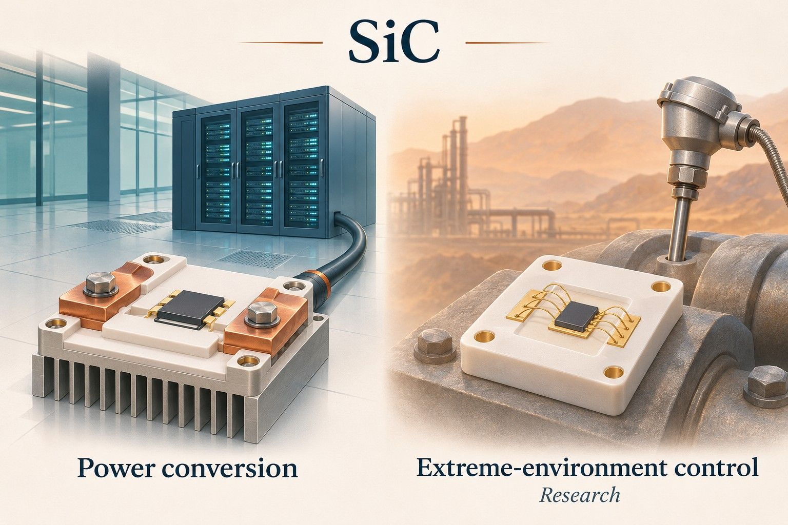
An AI server needs electricity before it can make a prediction. A sensor beside a hot machine needs electronics that remain functional before it can deliver useful data. Silicon carbide addresses both problems, through different devices. How far can this compound go: supplying an AI processor, extending the places where computation is possible, or becoming the computing element itself?
Silicon carbide, or SiC, combines silicon and carbon in a semiconductor with a wide energy gap and strong atomic bonds. Power transistors already exploit its electrical properties. Research also demonstrates logic gates, memory cells and artificial-neuron functions. The important distinction is between an established material, a working circuit and a complete AI system: progress in one does not automatically establish the others.[1][5][9]
One silicon atom, one carbon atom
The formula SiC expresses an equal number of silicon and carbon atoms in the ideal compound. It does not mean equal masses: using conventional atomic weights, the composition is approximately 70% silicon and 30% carbon by mass. Nor is SiC a mixture of two powders inside a chip. In its crystalline forms, each atom has four nearest neighbours of the other element. Different stacking sequences produce polytypes such as 3C, 4H and 6H, whose electrical properties differ.[1][2]
A typical Si–C bond is about 1.89 ångströms long, compared with about 2.35 ångströms for Si–Si in crystalline silicon. This is an atomic distance, not a transistor channel length or a manufacturing node. Shorter bonds do not, by themselves, make a processor smaller or faster. Circuit performance also depends on carrier transport, interfaces, geometry, contacts and wiring.[1]
For 4H-SiC, a bandgap of roughly 3.26 electronvolts, compared with about 1.12 for silicon, helps suppress thermally generated carriers. Its high critical electric field is valuable when a transistor must block a large voltage. Its thermal conductivity can help move heat through the material. These are distinct properties: tolerating temperature does not eliminate electrical losses, and conducting heat does not remove the need for a path from the device to its surroundings.[1]
Power reaches the AI chip through a chain
In a converter, a power transistor repeatedly switches current. Energy is lost both while it conducts and during transitions. SiC can reduce these losses in suitable high-voltage stages and support higher switching frequencies, allowing smaller magnetic components. The result depends on the complete design: gate drive, passive components, cooling, operating voltage and load all matter. A SiC switch is part of the power supply; it does not perform the accelerator’s matrix multiplications.[3]
NVIDIA’s published 800 V DC architecture illustrates the relevant opportunity. Higher distribution voltage reduces the current needed to deliver a given power, and the design seeks to avoid redundant conversion stages. The high-voltage distribution bus is followed by conversion near the computing equipment; it is not applied directly to a GPU’s logic. SiC manufacturers are developing components for this infrastructure, while the transition remains a system-level programme with protection, insulation and interoperability requirements.[3][4]
A simple calculation shows why the denominator matters. Suppose a converter continuously delivers 100 kW. At an assumed efficiency of 98%, it draws about 102.04 kW; at 99%, about 101.01 kW. The difference is approximately 1.03 kW. Converter losses have roughly halved, but total electrical input has fallen by about 1%. These are illustrative assumptions, not measured SiC performance or a forecast for a particular data centre.
For AI, the useful comparison is electricity per completed workload at equal output quality and response time, including the cooling that the power system requires. Lower conversion losses may release electrical and thermal capacity for computation. They do not prove that a model needs fewer arithmetic operations or that its GPU consumes less energy internally. This complements the collection’s discussion of gallium nitride and power conversion.
What has already been made to compute?
Tsinghua University researchers fabricated and tested 4H-SiC CMOS inverter and NAND gates using a six-inch wafer process compatible with power-device fabrication. Their transistors had 2 µm channels. The reported delays of 49.9 ns and 90 ns were calculated from measured inverter waveforms for the two output transitions. They are gate results, not the clock frequency or inference latency of a processor. The work also identifies unequal n-channel and p-channel threshold voltages, associated with the SiC–oxide interface.[5]
Memory is another necessary building block. A University of Arkansas, Fraunhofer IISB and Wolfspeed collaboration implemented six-transistor SRAM cells in a 1 µm SiC CMOS process and characterised them at 25 °C and 300 °C. High contact resistance affected the results. This establishes experimental storage circuitry, while leaving the density, capacity and peripheral circuitry of a practical memory system to be addressed. It supplies no basis for replacing the HBM beside an AI accelerator.[6]
NASA Glenn’s 2018 durability study goes beyond an isolated memory cell. A 16-bit RAM chip containing 195 SiC JFETs still read and wrote data after 10,100 hours—421 days—in air at 500 °C. Selected clock circuits also exceeded a year. These results concern particular fabricated circuits, interconnections and ceramic packaging; not every specimen reached the same duration. They are neither a temperature rating for every SiC device nor a neural-network demonstration.[7]
NASA’s processor: the design and the demonstration
The September 2026 NASA paper describes a one-bit control core with 2,463 SiC JFETs in a 5 × 5 mm layout. It can organise a transport-triggered architecture: moving data to a functional unit initiates that unit’s operation. Larger data words therefore need not be limited to the core’s one-bit Boolean decisions.[8]
The paper explicitly says the SiC design was awaiting successful fabrication. Its robot demonstration used a silicon FPGA proxy at room temperature. The quoted 0.15 W for the newer design, compared with 1.3 W for its predecessor at 500 °C, comes from simulation. Neither value measures a complete robot or an AI workload. The architecture is constrained towards simple control, with a clock below 100 kHz discussed in the introduction.[8]
For AI near a hot sensor, the prospective contribution is reliable acquisition, local decisions and communication with other processing stages. Demonstrating useful inference would additionally require suitable arithmetic, memory, a trained model and measured accuracy, latency and energy. Logical universality alone establishes none of those performance claims.
A colder route to artificial neurons
Researchers at the University of Hong Kong and collaborating US institutions demonstrated another use of SiC: artificial-neuron circuits operating at cryogenic temperatures. Their MOSFETs exhibit gate-controlled negative differential resistance, a region where voltage falls as current rises. Combined with circuit elements that accumulate and discharge charge, this produces sensory, logic and integrate-and-fire functions. The reported neuron demonstrations include device temperatures around 110–140 millikelvin.[9]
These experiments use discrete devices; peripheral components and measurement connections extend outside the refrigerator, and the demonstrated cascade uses a buffer amplifier. They support a route to neuromorphic circuitry, especially for already-cryogenic systems. They do not establish that cooling an ordinary AI server to those temperatures would save energy. Such a claim would require a complete task and the electricity consumed by refrigeration. The functional question connects to event-driven neuromorphic computing, but the operating conditions are very different.
Different results, different levels of readiness
| Route | Evidence | Remaining AI test |
|---|---|---|
| Power conversion | Industrial SiC components and proposed high-voltage data-centre architectures [3–4]. | Whole-system energy per equal-quality workload, across realistic loads. |
| Logic and memory | Fabricated gates and SRAM cells; separate high-temperature durability experiments [5–7]. | An integrated task with memory, interfaces and packaging under the same conditions. |
| NASA control core | SiC layout and simulations; functionality demonstrated through a silicon proxy [8]. | Fabricated SiC processor and application-level validation. |
| Artificial neurons | Cryogenic circuit functions and a two-stage cascade [9]. | Scalable networks, useful task accuracy and full refrigeration-inclusive energy. |
Other research broadens the material’s role. Tianjin University and Georgia Tech reported semiconducting epitaxial graphene on SiC: the electronically active graphene must not be confused with a SiC logic channel. Shanghai researchers and collaborators at the Technical University of Denmark reported a four-inch SiC-on-insulator photonic platform in November 2026. These are distinct routes towards electronic or optical functions, not independent confirmations of the NASA processor.[10][11]
Manufacturing announcements also need their proper scale. Infineon’s November 2026 report of functional power devices on a 300 mm SiC wafer concerns a power-semiconductor process milestone. It does not establish mass production of advanced SiC CPUs. Larger wafers, reliable interfaces, reproducible complementary transistors and durable interconnections address different obstacles; none substitutes for demonstrating the intended computation.[12]
The horizon is a division of functions
SiC deserves a place in AI hardware because electrical supply and operating environment constrain what computation can achieve. Its clearest current contribution is in power electronics. The more exploratory horizon is computation where conventional electronics struggle, together with specialised neuron and photonic devices.
The decisive next result would join those building blocks into a fabricated system that completes a defined task: the same sensing or inference problem, the required accuracy and response time, a specified temperature, and all relevant energy costs. Until then, the evidence supports extending the functions available to an AI system. It does not support announcing the disappearance of silicon processors.
Sources and scope
Evidence checked through 17 November 2026. Experimental papers, design studies and manufacturer announcements are distinguished above. The NASA processor paper was read in full, including its fabrication-status statement and the silicon-proxy demonstration. Corporate architecture documents describe their authors’ programmes, not independent AI-efficiency benchmarks.
- Ayalew, T. (2004). SiC Semiconductor Devices Technology, Modeling, and Simulation. TU Wien, §§2.1.1–2.1.2: crystallography and electrical properties. Material properties and polytypes; historical industrial data are not treated as current.
- Commission on Isotopic Abundances and Atomic Weights. Standard atomic weights of carbon and silicon. The approximate mass fractions above are calculated from 12.011 and 28.085.
- Kumar, A. (6 March 2026). Answering the Call: Powering AI with Reliable Silicon Carbide-Based Solid-State Transformers. Wolfspeed, technical white paper. Original document. Power-device applications and remaining system requirements; manufacturer perspective.
- Srivastava, N., & Petty, H. (13 October 2025). Building the 800 VDC Ecosystem for Efficient, Scalable AI Factories. NVIDIA Technical Blog. Architecture and technical white-paper access. Distribution and conversion are separated from processor logic supply.
- Yang, T., Wang, Y., & Yue, R. (2022). Demonstration of 4H-SiC CMOS digital IC gates based on the mainstream 6-inch wafer processing technique. Journal of Semiconductors, 43, 082801. doi:10.1088/1674-4926/43/8/082801. Fabrication, §2; measured switching waveforms and derived delays, §3, Fig. 7.
- Abbasi, A., Murphree, R., Roy, S., Suggs, M., Fraley, J., Mantooth, H. A., Di, J., & Erlbacher, T. (2019). High Temperature Memory Design, Implementation, and Characterization in 1 µm SiC CMOS Technology. HiTEN 2019, Oxford. Original paper. SRAM-cell measurements and contact limitations.
- Neudeck, P. G., et al. (2018). Year-long 500 °C operational demonstration of up-scaled 4H-SiC JFET integrated circuits. Journal of Microelectronics and Electronic Packaging, 15(4), 163–170. doi:10.4071/imaps.729648; NASA manuscript. Durability of fabricated circuits.
- Krasowski, M. J., Neudeck, P. G., Prokop, N. F., Adams, C. M., Greer, L. C., & Spry, D. J. (2026). Extreme Environment Durable Microprocessor Design Based on Silicon Carbide Junction Field Effect Transistor-Resistor Technology. IEEE Access, 14, 135548–135558. doi:10.1109/ACCESS.2026.3729473. §II-C/Fig. 5: layout and simulated power; §IV-C/Fig. 13: pending fabrication and silicon-FPGA robot demonstration.
- Yang, X., et al. (2026). Cryogenic neuromorphic circuits using gate-controlled negative differential resistance in silicon carbide. Nature Communications, 17, 4351. doi:10.1038/s41467-026-70963-6. Figs. 2–5 and Methods: neuron functions, temperatures, cascade and experimental connections.
- Zhao, J., et al. (2024). Ultrahigh-mobility semiconducting epitaxial graphene on silicon carbide. Nature, 625, 60–65. doi:10.1038/s41586-023-06811-0. Graphene-on-SiC material route.
- Zheng, Y., et al. (2026). 4H-silicon carbide integrated platform: from manufacturing to nonlinear photonics. Light: Advanced Manufacturing, 7, 114. doi:10.37188/lam.2026.114. Four-inch photonic platform; published 10 November 2026.
- Infineon Technologies (9 November 2026). Infineon marks innovation milestone with world’s first 300-millimeter power silicon carbide wafer. Manufacturer announcement. Functional power devices; priority claim belongs to the manufacturer.
Continue exploring Horizons of Electronics.
Liked this post? Follow this blog to get more.