A matrix multiplication on an AI chip passes numbers from one arithmetic unit to its neighbour. Look inside either unit and the same pair of switches appears again and again. What would change if those two switches could share a patch of silicon?
A complementary field-effect transistor (CFET) places an n-type transistor above or below its p-type partner. Circuits built this way can already invert a signal, sustain an oscillation and store a bit. For AI, the interesting question comes one scale higher. Bringing thousands of logic gates closer together can shorten the wires between them. Whether that saves energy depends on how fast those gates run, how much heat they generate and how often they wait for data. [1], [3], [4]
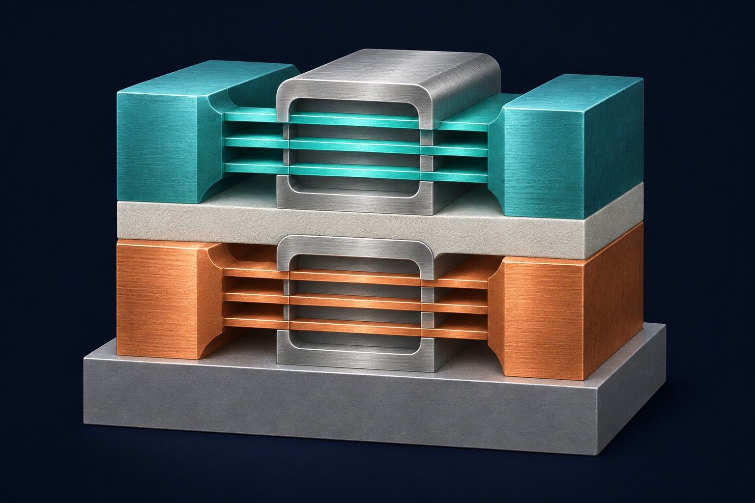
What changes when the two switches share a footprint?
Consider an inverter, the circuit that turns a low input into a high output and a high input into a low output. At a low input voltage, its p-type transistor connects the output to the supply. A high input turns on the n-type transistor and pulls the output towards ground. The same circuit can be built with the two devices side by side or with one above the other. The vertical arrangement takes out some of the lateral distance between them. The designer must still find space for the contacts that connect each device to the rest of the circuit. [1], [2]
In a nanosheet transistor, a gate wraps around thin semiconductor channels to control the current. Several sheets can belong to a single transistor. The distinctive step in a CFET is stacking the complementary devices themselves. Repeated across a chip, this can make the standard cells, the small reusable layouts for functions such as logic gates, narrower in one direction. A shorter wire between cells can carry less capacitance to charge and discharge at each transition. Inside an individual cell, however, tighter spacing and the connections to the lower tier can add capacitance and resistance. The two effects act at different scales. [2], [4]
What has actually worked in silicon?
At IEDM 2023, Intel reported a functioning stacked CMOS inverter with backside device contacts. Its most tightly spaced devices had three n-type nanoribbons above three p-type nanoribbons, with 30 nm of vertical separation. The reported 60 nm gate pitch measures the repeating distance between gates along the wafer. Those two numbers describe different directions in the device. [1]
In 2024, imec electrically tested complementary devices with a common gate and separate upper and lower source/drain contacts reached from the front of the wafer. Its test structure had an 18 nm gate length, a 60 nm gate pitch and 50 nm of vertical separation. This also clarifies the link with PowerVia, explored earlier in this collection. PowerVia changes the route the supply current takes into the logic. CFET changes where the two transistors sit. The Intel inverter combined these ideas. The imec test shows that a stacked pair can operate with frontside contacts as well. [1], [2]
At IEDM 2025, TSMC reported a 101-stage CFET ring oscillator and functioning static random-access memory (SRAM) bit cells at a gate pitch below 48 nm. In a ring oscillator, a transition travels through a chain of inverting stages and returns to the beginning, causing the circuit to switch repeatedly. A memory cell tests another property, the ability to maintain a stable state. Together they establish that stacked devices can be connected into working circuits. Transferring that result to a useful cache requires a whole array, its read and write circuitry, and evidence that enough cells work across a wafer. [3]
What would an AI accelerator gain?
A 2026 preprint follows one specific design far enough to give a quantitative answer. The authors laid out the same 32 × 32 array of multiply-and-accumulate units twice. These units pass operands between neighbours and accumulate partial sums, as in the matrix products used by neural networks. One layout used a lateral nanosheet library called A10, the other a stacked CFET library called A7. The study used the same intrinsic transistor model, metal routing stack and proportion of occupied layout area for the comparison. Both implementations were computer models. [4]
After placing the cells and routing the wires, the CFET array occupied about 25% less area and used 12% less total wire length. At the same supply voltage of 0.8 V, the authors calculated a higher attainable clock rate. Running at the resulting design frequencies also raised estimated total power by 75%. In a separate comparison, they lowered the CFET supply voltage until the two designs ran at the same frequency. Under those assumptions the CFET design drew less power. The difference matters to a chip designer deciding whether to spend a timing gain on more operations per second or on a lower operating voltage. [4, Fig. 7, Table II and Fig. 8]
Consider two stages of language-model inference. A large batch of input tokens can keep a matrix engine busy. Shorter paths through that engine could help it finish those products sooner if memory supplies operands fast enough. When generating one token at a time for a single user, fetching model weights can occupy much of the interval. Shortening a wire inside a multiplier leaves those off-chip bytes to be fetched. Extra logic density also concentrates heat if the available area is filled with simultaneously active units. These are reasons to measure the whole accelerator at its sustained operating point. [4], [5]
What would settle the question?
A convincing comparison would run the same model at the same numerical precision and output quality, with matched memory bandwidth, batch size, context length and cooling. For prompt processing, report input tokens per second and time to the first output token. During generation, record time between tokens and joules per output token at the system power input. If a denser array wins on matrix arithmetic while those application measures stay flat, the result identifies where the next constraint lies. CFET research has already established functional stacked logic and one-bit storage. Its strongest AI result so far in the studies examined here is a shorter, denser modelled compute array. The application-level energy and latency gains remain open experimental questions.
Sources and scope
Evidence reviewed through 17 November 2026. The first three sources describe fabricated devices or circuits. The fourth estimates circuit and chip behaviour from physical layouts. The final source supplies the inference context for the comparison.
- M. Radosavljević et al., Intel (2023). Demonstration of a Stacked CMOS Inverter at 60nm Gate Pitch with Power Via and Direct Backside Device Contacts. IEEE International Electron Devices Meeting, paper 29.2. Device cross-sections and electrical measurements.
- imec (2024). Imec demonstrates functional monolithic CFET devices with stacked bottom and top contacts. Research institute report accompanying the IEEE Symposium on VLSI Technology and Circuits, 18 June. Figures 1 and 2 show the contacts and measured transistor characteristics.
- S. S. Liao et al., TSMC (2025). First Demonstration of CFET Ring Oscillator and SRAM Bit-Cell Functionality at Gate Pitch Smaller Than 48 nm for Future Logic and SRAM Technology. IEEE International Electron Devices Meeting, paper 2.5. The conference abstract describes the oscillator and memory cells.
- M. Benkhelifa et al. (2026). System-Technology Co-Evaluation of A7 CFET and A10 NSFET Technologies from Cell Parasitics to Chip Reliability. arXiv:2609.15326v1, 14 September. Section III-B, Figures 7–8 and Table II specify the array, baseline and voltage comparisons.
- R. Pope et al. (2022). Efficiently Scaling Transformer Inference. arXiv:2211.05102. Analysis and experiments on the compute and memory demands of Transformer inference.
Liked this post? Follow this blog to get more.