Suppose a transistor in an AI processor is meant to be off. Its drain is still connected to the circuit, and the voltage there can draw charge through a very short channel. How can the gate retain control as the distance between source and drain shrinks?
Intel’s RibbonFET answers that question by wrapping a gate around each of several thin silicon ribbons. The ribbons share a source and a drain and carry current in parallel. This geometry gives a designer more control over leakage and a choice of channel widths. Both matter in a matrix engine that switches millions of gates, especially if it can complete the same work at a lower supply voltage. A measurement on a working CPU shows how much the power supply itself matters to that promise. [1] [2]
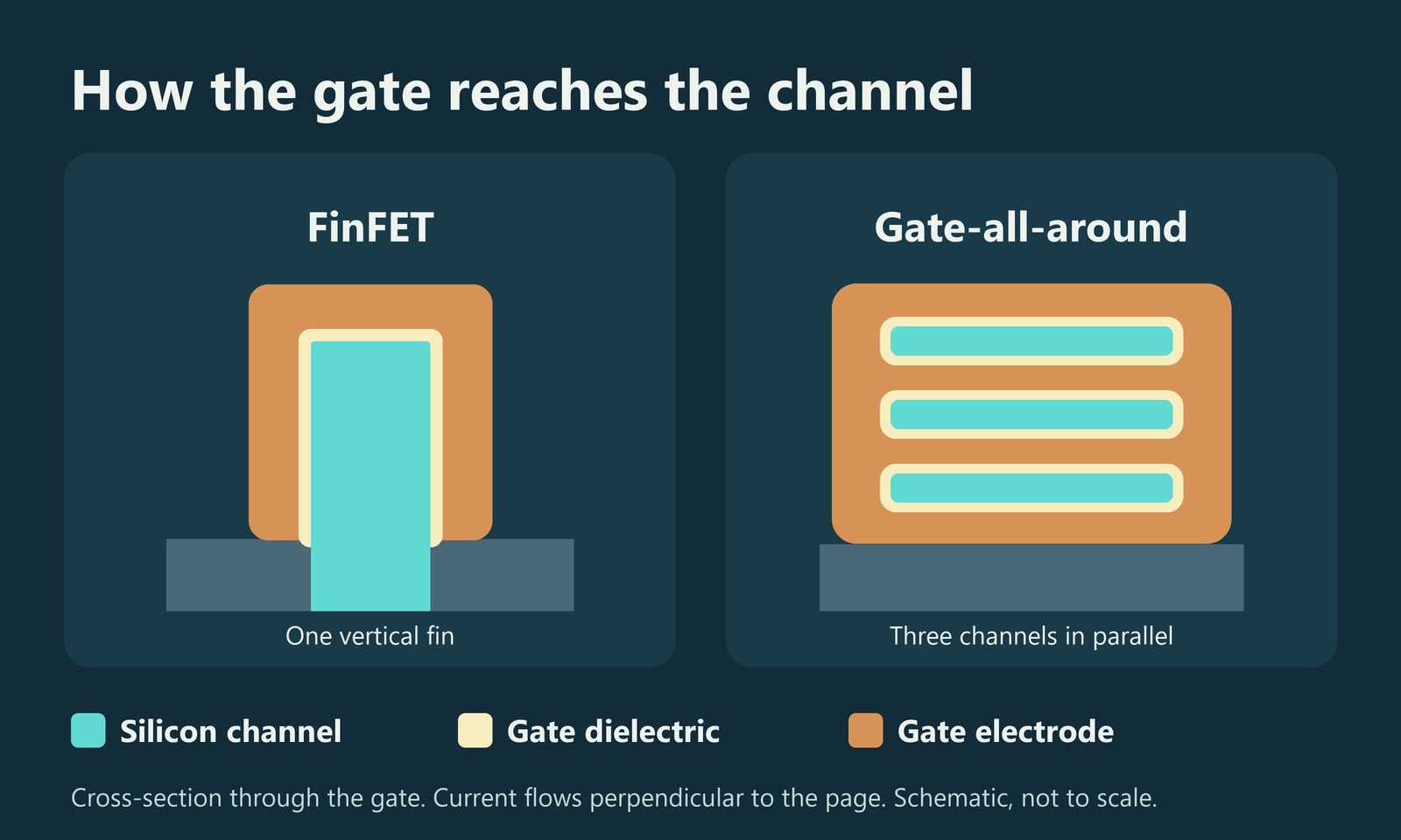
What changes when the gate reaches underneath?
The gate controls the energy barrier that carriers must cross to travel from source to drain. An insulating film lets its electric field act on the silicon while keeping the gate electrode electrically separate. In a typical tri-gate FinFET, the channel is an upright fin. The gate acts from the top and the two sides. As the channel gets shorter, the drain gains influence over the barrier at the source. Current can then flow even when the gate voltage calls for the transistor to stay off. [1]
In a gate-all-around (GAA) nanosheet transistor, the silicon extends horizontally in thin sheets. The gate reaches the underside as well as the top and edges of every sheet. Several channels fit within one footprint. There is another advantage for circuit designers. In a process with fixed fin dimensions, adding drive current generally means adding a whole fin. Nanosheet designers can also vary sheet width within the choices supported by the process. A wide device might drive a long wire or several following gates. A smaller device can spare the previous stage some capacitance to charge. The best choice depends on the load. [1]
What did the first devices actually measure?
A team from IBM, Samsung and GlobalFoundries reported electrical measurements on three-sheet transistors in 2017. Each silicon sheet was 5 nm thick and the gate length was 12 nm. For an n-type device at a 44 nm gate pitch, the best reported subthreshold swing was 75 mV per decade. Gate pitch is the repeat distance between adjacent gates. Gate length and sheet thickness measure different features. [1]
Subthreshold swing answers a practical question about the switch. In the measured region just below threshold, changing the gate voltage by about 75 millivolts changed the current by a factor of ten. A smaller swing gives a circuit designer a steeper transition over this range. The value describes that device under its test conditions. Estimating energy in a complete circuit also requires its load, supply voltage, leakage and time spent switching. Fabrication matters too. The team had to remove material selectively from between the sheets while preserving the thin silicon that would carry the current. [1]
Where do RibbonFET and PowerVia meet?
At the 2026 VLSI Symposium, Intel reported silicon measurements on CPU cores using GAA transistors and backside power delivery. At around 0.5 V, the cores reached approximately 30% higher frequency than the FinFET designs in the comparison. Intel attributes the result to a lower transistor threshold voltage and a smaller voltage drop between the supply and the working circuit. Both changed in the experiment. Its result establishes a frequency advantage for those cores at that low-voltage operating point. The study gives no separate percentage for the contribution of RibbonFET alone. [2]
The distinction is visible in two earlier instalments. PowerVia brings the supply through the back of the chip. In TSMC A16, we followed that supply towards a nanosheet device. Here we have followed the electric field from the gate to its channel. The CFET article goes one step further in the vertical direction by placing a complete n-type transistor above or below its p-type partner.
Which chips have made the transition?
RibbonFET is Intel’s name for its ribbon implementation. Samsung announced initial production of its 3 nm GAA process, called MBCFET, in 2022. TSMC reports that its first-generation N2 nanosheet process entered volume production in the fourth quarter of 2025. Intel launched its Core Ultra Series 3 family built on Intel 18A in January 2026. FinFET remains in production in other families, including TSMC N3. These milestones establish industrial use. Different products, circuits and manufacturing processes prevent a like-for-like ranking of the three transistor implementations from these announcements. [3] [4] [5]
When would a model use less energy?
Consider a matrix engine processing many input tokens together. If the operands arrive on time and the engine can sustain its clock at lower voltage, each transition can cost less energy. At equal switched capacitance, dynamic energy scales approximately with the square of the supply voltage. A chip’s total also includes leakage, memory traffic and power conversion. During single-user generation, fetching the weights for the next token can consume a large part of the time between tokens. Raising the arithmetic clock does little for a unit that is waiting for memory. [6]
A decisive comparison would hold model quality, numerical precision, context length, batch size, memory bandwidth and cooling constant. Measure time to the first token for prompt processing, then time between output tokens and system joules per output token during generation. The device evidence establishes tighter control over a short channel, and the Intel experiment shows a measurable benefit at low voltage for an entire core with backside power. How much of that benefit reaches an AI user depends on where the workload spends its time and energy.
Sources and scope
Evidence reviewed through 17 November 2026. Device transfer curves, CPU frequency measurements and manufacturer production statements answer different questions. The inference study supplies the workload context.
- N. Loubet et al. (2017). Stacked nanosheet gate-all-around transistor to enable scaling beyond FinFET. Symposium on VLSI Technology. Figures 3–6 examine device sizing and circuit design. Figure 11 shows measured devices and transfer characteristics.
- M. Shamanna et al., Intel (2026). CPU Cores in GAA with Backside Power: Silicon-Validated Design Insights. IEEE/JSAP Symposium on VLSI Technology and Circuits, T2.3. See also figure 3 of the Intel 18A process brief for the low-voltage comparison. Intel’s technical account of the measured CPU cores.
- Samsung Electronics (2022). Samsung Begins Chip Production Using 3nm Process Technology With GAA Architecture. Initial production and adjustable channel width.
- TSMC. 2nm Technology. Foundry process description and start of N2 volume production.
- Intel (2026). CES 2026: Intel Core Ultra Series 3 Debuts as First Built on Intel 18A. Commercial product announcement, 5 January.
- R. Pope et al. (2022). Efficiently Scaling Transformer Inference. Controlled inference experiments and analysis of compute and memory demands.
Liked this post? Follow this blog to get more.